Study how the encoded binary (machine code) is passed to the processor
Building a Processor: Datapath & Controlpath
Two main components for a processor: Datapath and Controlpath
Datapath
- collection of components that process data
- performs the arithmetic, logical and memory operations
Controlpath
- tells the datapath, memory and I/O devices what to do according to program instructions
MIPS Processor: Implementation
Let’s try to implement a subset of the core MIPS ISA!
Arithmetic: add, sub, and, or, addi, slt
Data transfer instructions: lw, sw
Branches: beq, bne
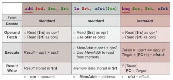
Instruction Execution Cycle
A MIPS instruction is executed in different stages. The following is a simplified overview:
- Fetch
- Get instruction from memory
- Address is in Program Counter (PC) register (of the next instruction)
- Decode
- Find out the operation required
- e.g.
add $s0, $s1, $s2
- Operand Fetch
- Get operand(s) needed for operation
- e.g.
$s1and$s2
- Execute
- Perform the required operation
- e.g
$s1 + $s2
- Result Write (Store)
- Store the result of the operation
- e.g. store result to
$s0
MIPS Instruction Execution
An example of what happens to different instructions
For the sake of simplicity, we will merge the decode and operand fetch operation. i.e
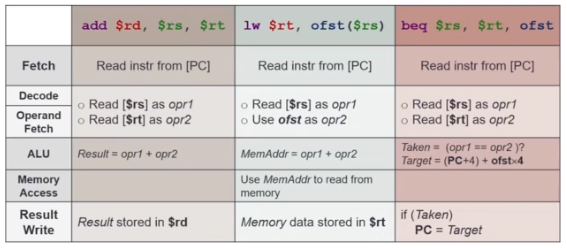
- Merge Decode and Operand Fetch
- Execute is split into ALU and Memory Access
Let’s Build a MIPS Processor
Fetch Stage
- Use the PC (special register in the processor) to fetch the instruction from memory
- Increment the PC by 4 bytes to get the address of the next instruction
- increment by 4 because each instruction is 32 bits
- EXCEPTIONS: branch/ jump instructions
Elements
Instruction Memory
- input: address
- output: content (instruction) at the address
Adder:
- input: A, B (where both A and B are 32-bit numbers)
- output: sum of the numbers, A+B
Clocking
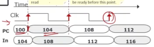 It seems that the PC is being read and written at the same time. How do we ensure that we read, then write?
- PC is read during the first half of the clock period
- PC is then updated with PC+4 at the next rising clock edge
For example 3.2 GHz processor
- 3.2 billion square waves/ second (frequency)
- is responsible for timing the operations inside the processor
Decode Stage
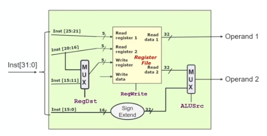 Determines what to do after receiving 32-bit binary instruction
- Read
opcodeto determine instruction type and field length - Read data from all the necessary registers
Elements
Register File
- read at most two registers per instruction
RegRead: returns the two registers that are to be read from
- write at most one register per instruction
RegWrite: (boolean) returns whether or not to write the data given into the write register. 0 False, 1 True
Multiplexer (MUX in the diagram)
- input: n inputs
- output: choose 1 of the input depending on the Control Signal
- Control Signal is represented with bits
- For example
- There are only 2 inputs, A or B
- The
RegDstis 0 or 1 - If 0 → return A
- If 1 → return B
Decode R-Format Instructions
e.g. add $8, $9, $10 (but in binary)
Uses the multiplexer with Control Signal:
RegDst= 1- For choosing
rdto be on the write register
- For choosing
AlUSrc= 0- For choosing Read Register 2 to be the second output to the ALU Register File
- Read Register 1:
$9 - Read Register 2:
$10 - Write Register:
$8 - Write Data: not defined yet (will store output of the ALU Stage)
- Outputs register 1 and register 2 to the ALU Stage
Decode I-Format Instruction
e.g. addi $21, $22, -50 (but in binary)
- Also applies for
lwinstruction - A little different for branch instructions, e.g.
beq,bneUses the multiplexer with Control Signal: RegDst= 0- For choosing
rtto be on the Write Register
- For choosing
AlUSrc= 1 (EXCEPT FOR BRANCH INSTRUCTIONS,AluSrc = 0)- For choosing immediate value to be the second output to the ALU
- Sign extension done to the immediate value (16 bit → 32 bit) Register File
- Read Register 1:
$22 - Read Register 2:
$21(** rt value is passed to read register 2 first! ) - Write Register:
$21- made possible due to a multiplexer
- Write Data: not defined yet
- will store output of the ALU Stage
- Outputs register 1 and immediate value to the ALU Stage
- Made possible due to a multiplexer
- immediate value (16 bit) is converted into 32bit using Sign extension
ALU Stage/ Execution Stage (Ex)
- performs instructions given operation, operand 1 and operand 2 from the Decode Stage
- Arithmetic Operations
- Memory Operations
- Branch Operations
Elements
Arithmetic Logic Unit (ALU)
- input: two 32-bit long operands
- output: 32-bit long ALU result
- isZero` control signal
- 1 if A op B = 0
- 0 if A op B != 0
- isZero` control signal
ALUcontrol- 4-bit
- Tells what type of operation the ALU needs to perform
- Set using opcode/ funct
Performing Branch Instructions
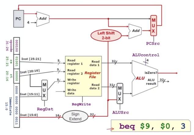 Arithmetic instructions can be easily performed, but branch instructions are harder to perform. Two calculations would have to be performed
e.g.
Arithmetic instructions can be easily performed, but branch instructions are harder to perform. Two calculations would have to be performed
e.g. beq $9, $0, 3
- Branch Outcome
- use ALU to compare registers
- Branch Target Address
- Uses Control Signal with the multiplexer
PCSrc- 0: (PC + 4)
- 1: PC + 4 + immediate * 4
- Introduce additional logic to calculate the address
- need PC (from Fetch Stage)
- need Offset (from Decode Stage)
- PC = PC + 4 + immediate * 4
- Uses Control Signal with the multiplexer
Memory Stage
Only lw and sw instructions need to perform operations in this stage
- Input: memory address from ALU Stage/ Execution Stage (Ex) (if computation is required) or Decode Stage
- Output: Result to be stored (if applicable)
- Read and Write control signals present:
MemWrite,MemRead- if write = 1 and read = 0, data will be written to the memory address
- if write = 0 and read = 1, data from the address will be passed to “Read Data”
- if write = 0 and read = 0, nothing happen
- if write = 1 and read = 1, SHOULD NOT happen!
Different from Instruction Memory
Fetch Stage fetches the instruction memory from the RAM while this stage fetches program data from the RAM.
Elements
Data Memory
- Address
- Write Data
Examples
e.g. lw $21, -50($22)
- ALU will give the calculated address from
-50($22) MemWrite= 0,MemRead= 1- Data Memory will read data from
-50($22)and pass it as an output
e.g. sw $21, -50($22)
- ALU will give the calculated address from
-50($22) - Decode Stage will give the address
$21 MemWrite= 1,MemRead= 0- Data Memory will read data from
$21and write the data into-50($22)
Register Write Stage
writes the result of computations to a register in this stage.
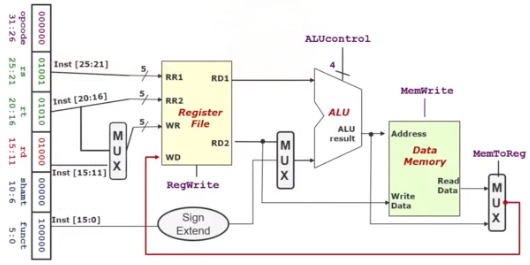
- Requires:
- destination register number
- Taken from Decode Stage
- data to write into dest register
- either from ALU Stage/ Execution Stage (Ex) or Memory Stage
- Decided to
MemToRegcontrol signal of a Multiplexer
- destination register number
- sets
RegWriteof the RegisterFile (see Decode Stage) to write the data into the “write register”