Introduction
Combinational Circuit
- Output depends entirely on the immediate inputs
Sequential Circuit
- Each output depends on both present inputs and state
- two types
- Synchronous
- Asynchronous
- Multivibrator
- Bistable (We will only be looking at this)
- Latches and flip-flops
- They differ in the methods used for changing their state
- Monostable or one-shot
- Astable
- Bistable (We will only be looking at this)
Memory Elements
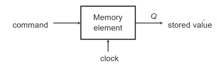
A device which can remember value indefinitely, or change value on command from its inputs. (as long as the power is on)
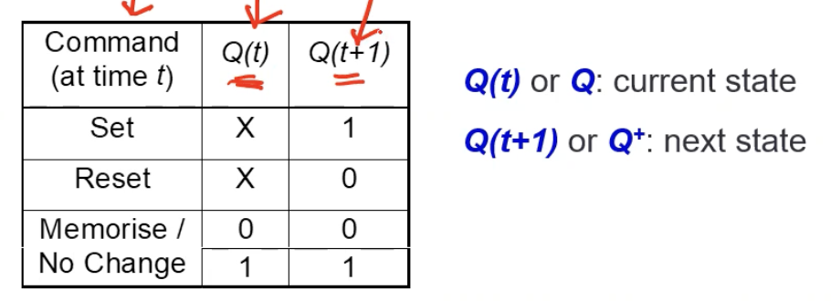
Characteristic Table
GH### Memory Elements with clock
- the command is only effective at a particular time (i.e. rising edge of a clock cycle)
- Two types of triggering
- Pulse-triggered (high/ low level)
- Latches
- ON = 1, OFF = 0
- Edge-triggered (rising/ falling edge)
- Flip-flops
- Positive edge-triggered (ON = 0 → 1, OFF = others)
- Negative edge-triggered (ON = 1 → 0, OFF = others)
- Pulse-triggered (high/ low level)
Latches
- Two inputs: S and R (set and reset)
- Two complementary outputs: Q and Q’
- When Q = High, we say latch is in SET state
- When Q = Low, we say latch is in RESET state
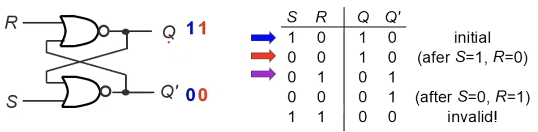
- For active-high input S-R latch (also known as NOR gate latch)
- R = HIGH and S = LOW → Q becomes LOW (RESET state)
- S = HIGH and R = LOW → Q becomes HIGH (SET state)
- Both R and S are LOW → No change in output Q
- Both R and S are HIGH → Outputs Q and Q’ are both LOW (invalid state! )
- Drawback: invalid condition exists and must be avoided
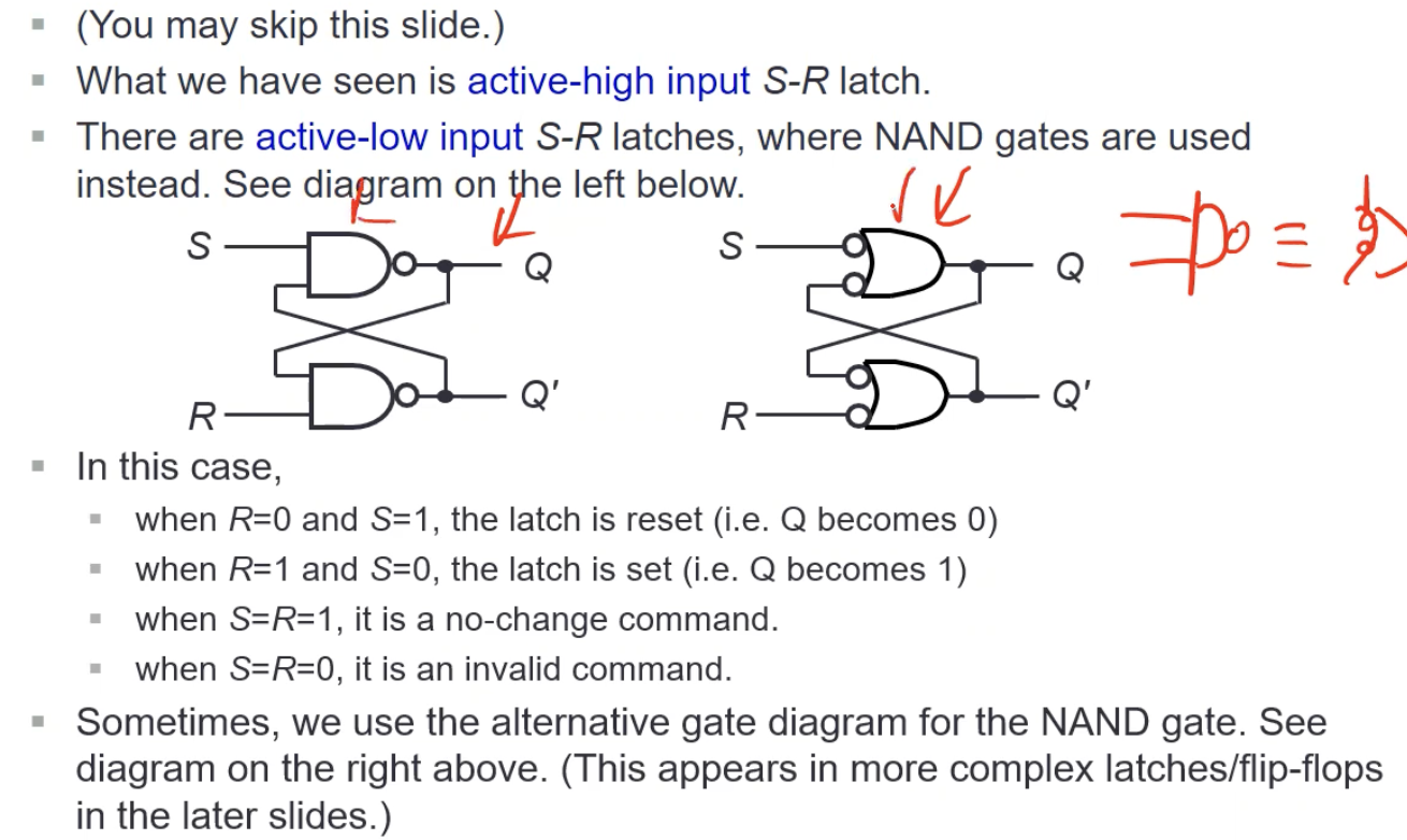
Active-high input S-R latch:
Active-low S-R Latch
Active-low is 0 state activated where Active-high is 1 state activated
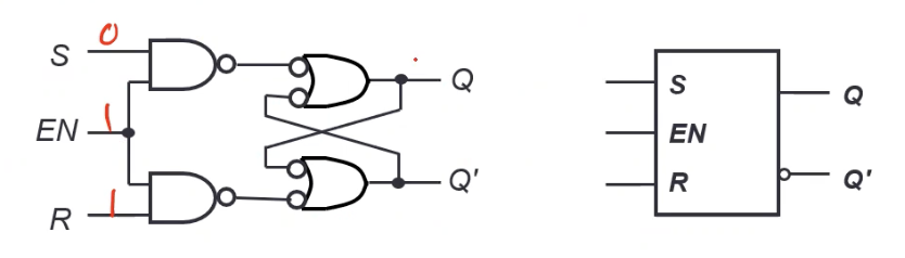
Gated S-R Latch
S-R Latch + enable inputs (EN) and 2 NAND gates
- Outputs change only when EN is high
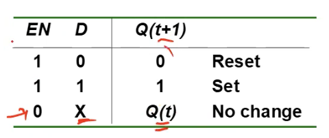
Gated D Latch
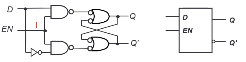
- Eliminates the undesirable condition of invalid state in the S-R latch
- Characteristic table
Flip-Flops
Synchronous bistable devices
- output changes state at a specified point on a triggering input called the clock
- Enable input becomes a clock!
>denotes edge triggered device
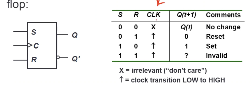
S-R Flip-flop
- Characteristic table of positive edge-triggered S-R flip-flop:
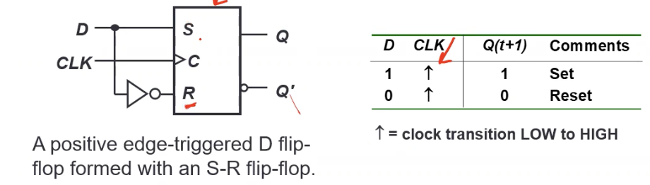
D Flip-flop
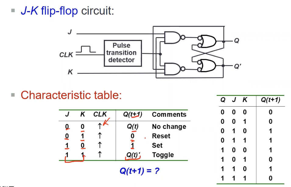
J-K Flip-flop
- Q and Q’ are fed back to the pulse-steering NAND gates.
- No invalid state
- Include a toggle state
- J = HIGH and K = LOW → Q becomes HIGH (SET state)
- K = HIGH and J = LOW → Q becomes LOW (RESET state)
- Both J and K are LOW → No change in output Q
- Both J and K are HIGH → Toggle
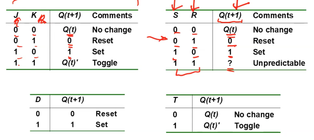
Characteristic table
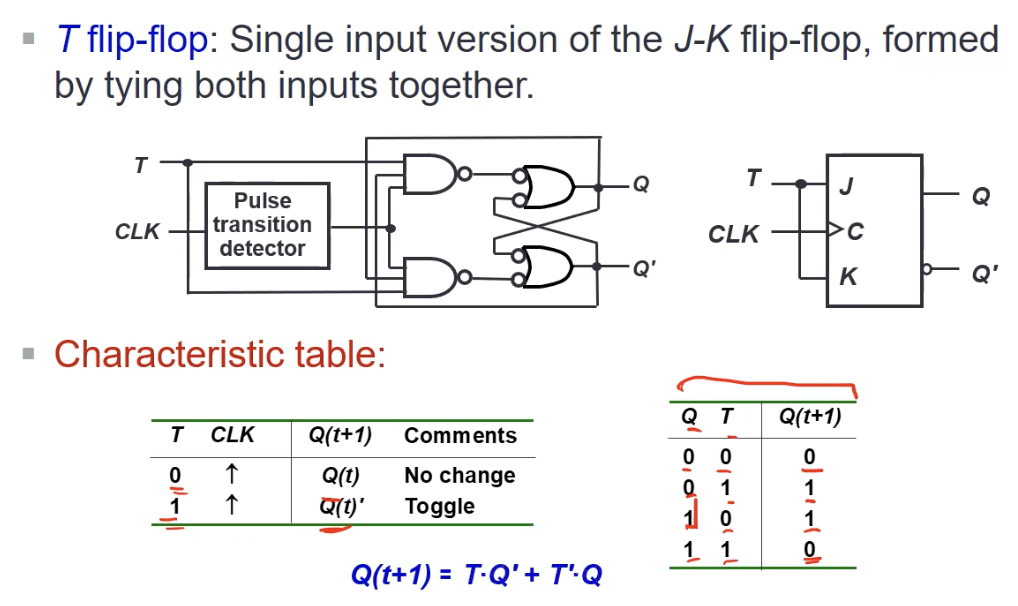
T Flip-flop
Single input version of the J-K flip-flop, formed by tying both inputs together
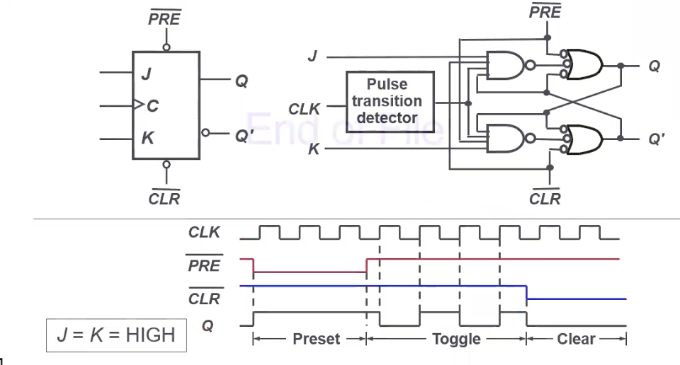
Asynchronous Inputs
- S-R , D and J-K inputs are synchronous inputs, as data on these inputs are transferred to the flip-flop’s output only on the triggered edge of the clock pulse
- Asynchronous inputs affect the state of the flip-flop independent o the clock;
- e.g. preset (PRE) and clear (CLR)
- When PRE = HIGH, Q is immediately set to HIGH
- When CLR=HIGH, Q is immediately set to LOW
- Flip-flop in normal operation mode when both PRE and CLR are LOW
Synchronous Sequential Circuit
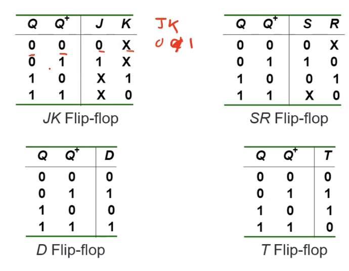
Flip-flop characteristic tables (Summarise)
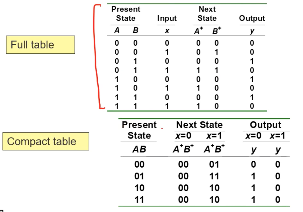
Analysis
- Given a sequential circuit diagram, analyse behaviour by deriving
- state table
- state diagram
- State Equations
- Output Functions
- We use
A(t)andA(t+1)or simplyAandA+to represent the present state and the next state, respectively, of a flip-flop represented by A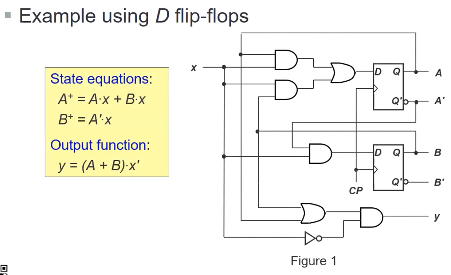
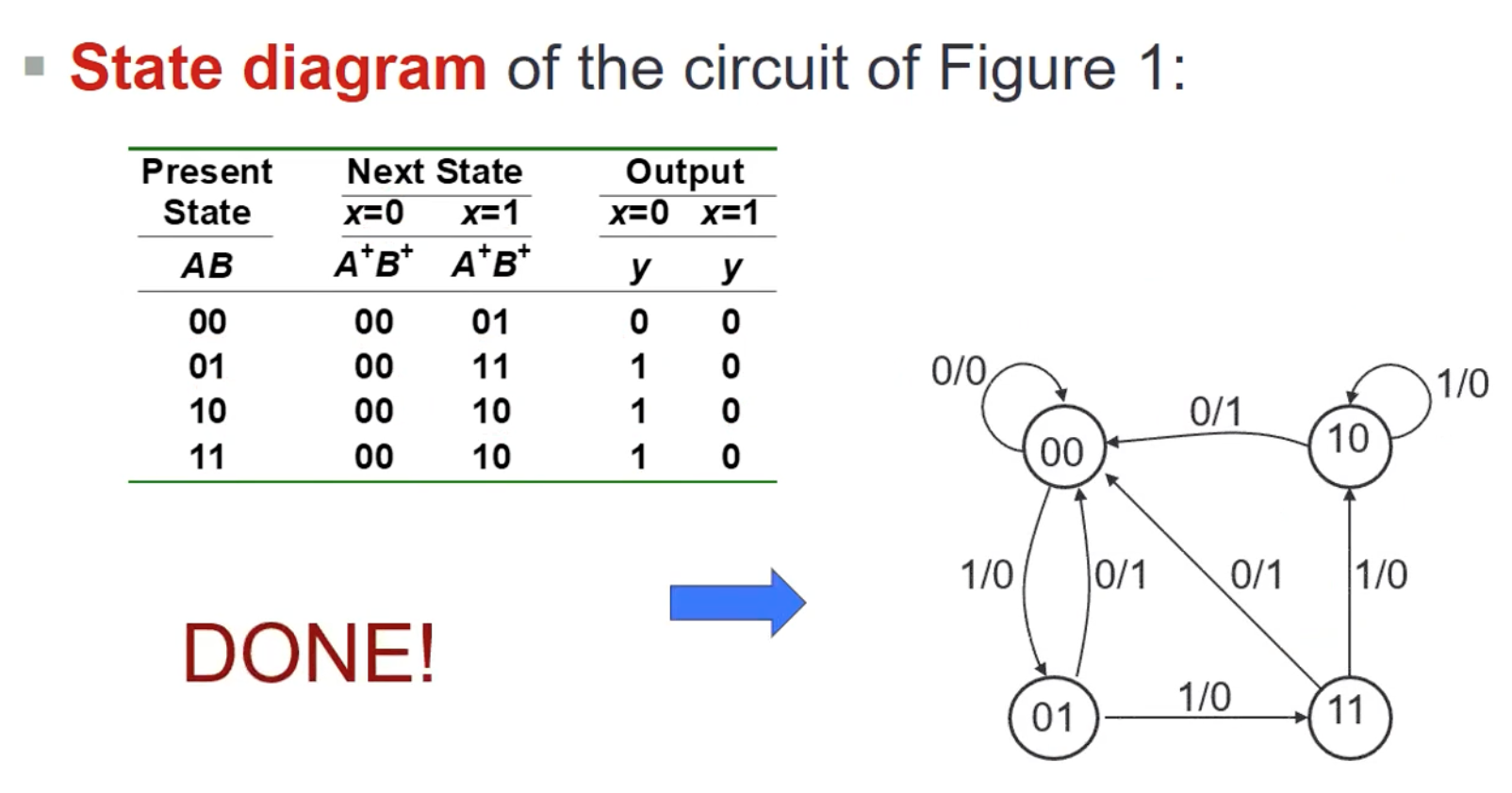
- from state table, we draw the state diagram
- state is denoted by a circle
- Each arrow denotes a transition of the sequential circuit (a row in state table)
- A label of the form a/b is attached to each arrow where a denotes the inputs while b denotes the outputs of the circuit in that transition
- m flip-flops → up to states
Excitation Tables
- given the required transition from present state to next state, determine the flip-flop input(s)
Memory
Definitions
- 1 byte = 8 bit
- 1 word
- multiple of bytes
- a unit of transfer between main memory and register
- usually the size of the register
- 1 KB = 2^10 bytes
- 1 MB = 2^20 bytes
- 1 GB = 2^30 bytes
- 1 TB = 2^40 bytes
- Desirable properties
- fast access
- large capacity
- cheap
- non-volatile
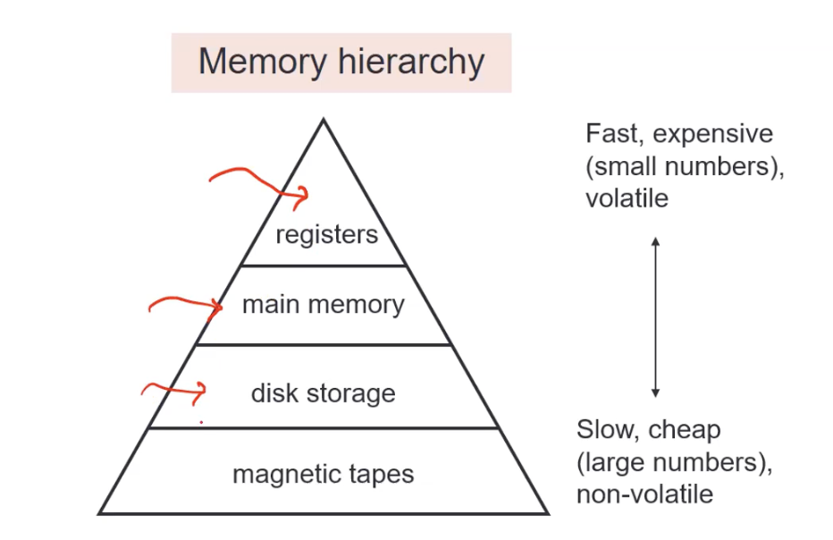
Memory Hierarchy
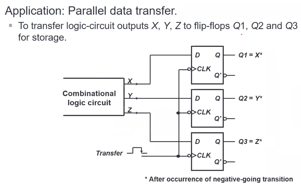
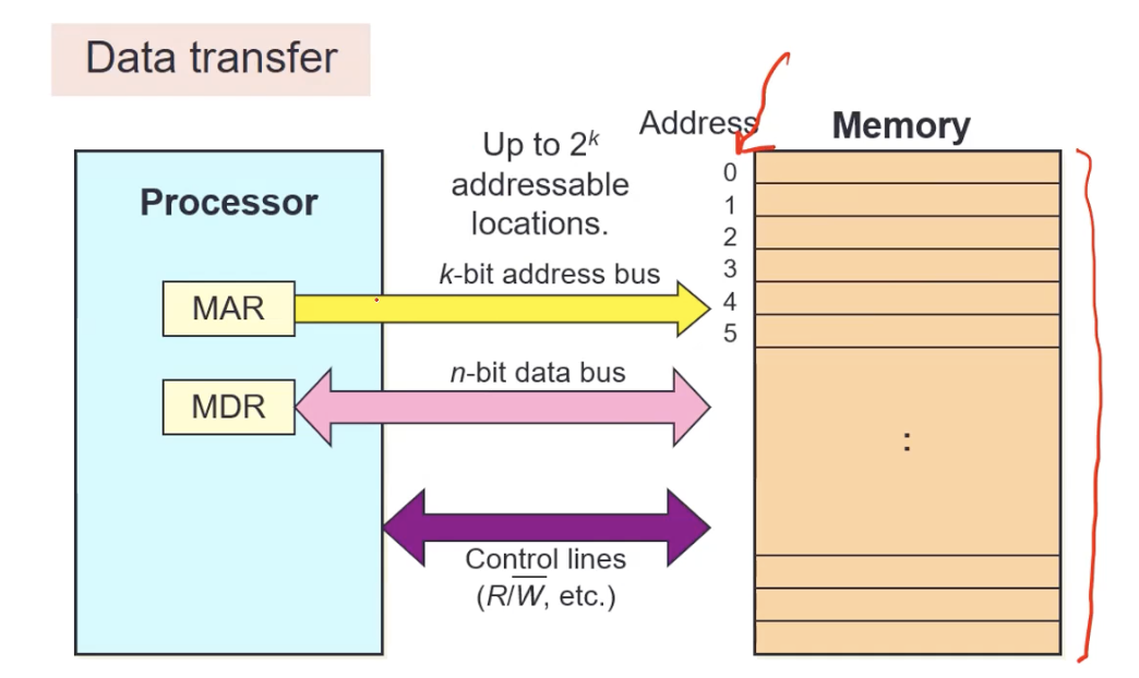
Data transfer
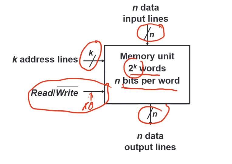
Memory Unit
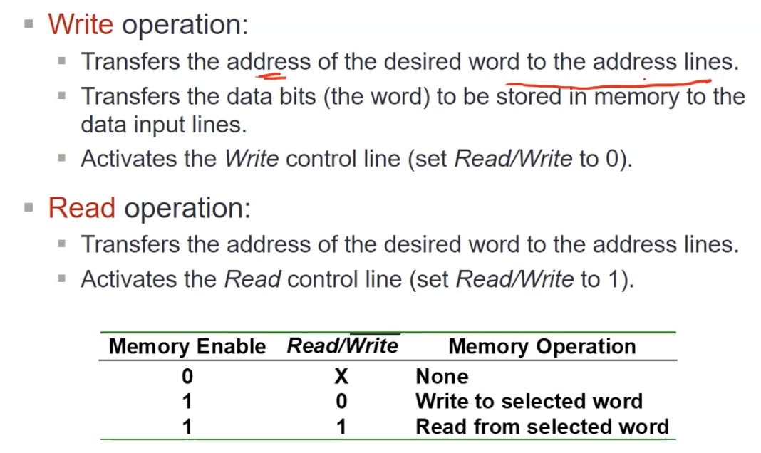
Read/ Write Operations
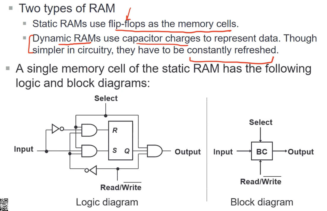
Memory Cell