Introduction
Combinational Circuits
- Each output depends entirely on the immediate present (inputs)
Sequential Circuit
- Each output depends on both present inputs and state
Analysis Procedure
- Label the inputs and outputs
- Obtain the functions of intermediate points and the outputs
- Draw the truth table
- Deduce the functionality of the circuit
Design Methods
Different methods
- Gate-level (with logic gates)
- Block-level (with functional blocks)
Main Objectives
- Reduce cost
- increase speed
- Design simplicity
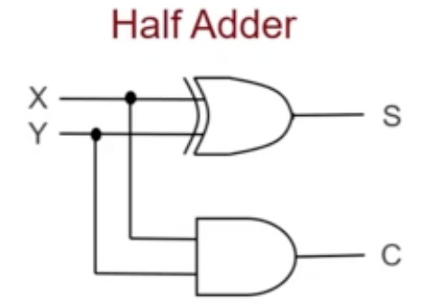
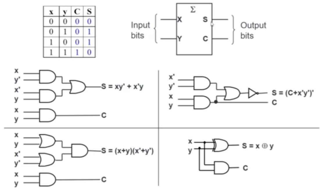
Gate-Level (SSI) Design: Half Adder
- State Problem → Half Adder
- Determine and label the inputs and outputs of the circuit
- Draw the truth table
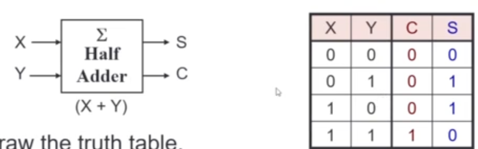
- Obtain simplified Boolean Functions (can use K-Maps!)
- e.g.
- Draw logic diagram
Block-Level Design
More complex circuits can also be built using block-level method.
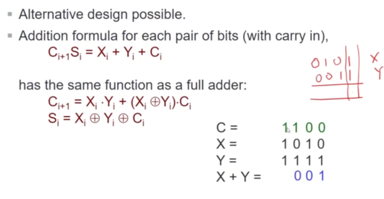
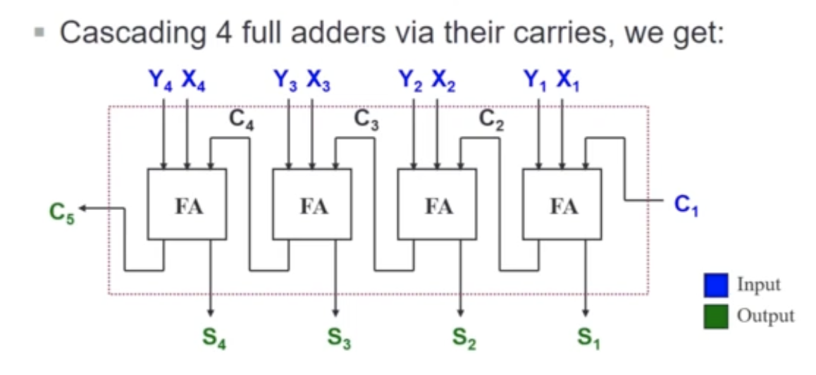
- Generally, block-level design method relies on algorithms or formulae of the circuit, which are obtained by decomposing the main problem to sub-problems recursively
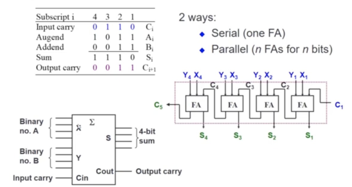
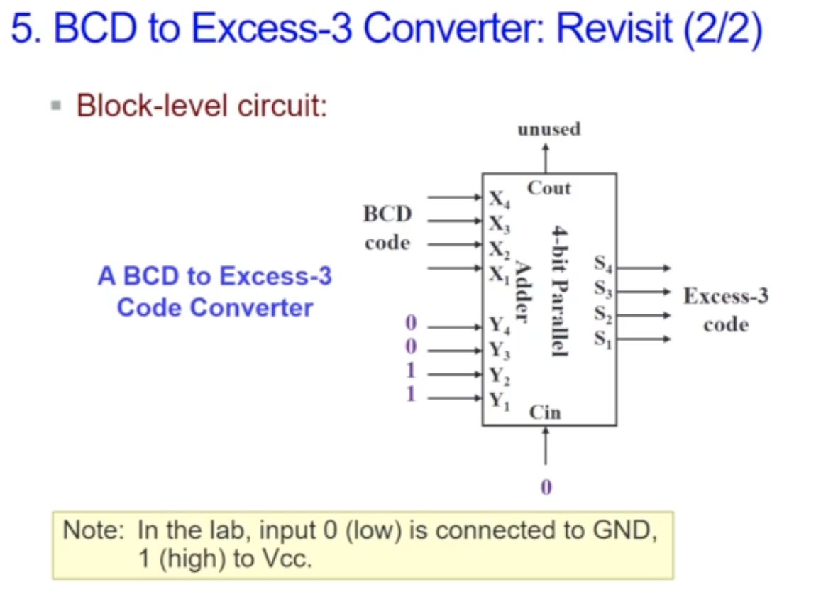
4-bit Parallel Adder
- Circuit to add two 4-bit numbers together and a carry-in, to produce a 5-bit result
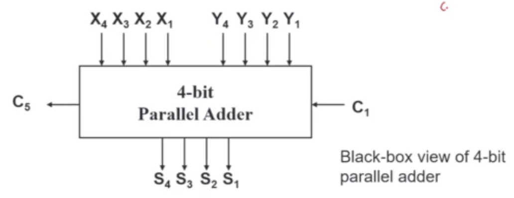
- If you were to try to construct the truth table, you realise that it is too big, there are rows!
- Simplification becomes too complicated!
- We note that we can obtain Excess-3 code with the parrallel adder
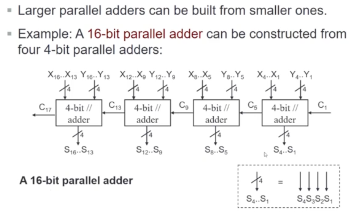
- You can also build a 16-bit parallel adder with a 4-bit parallel adder!
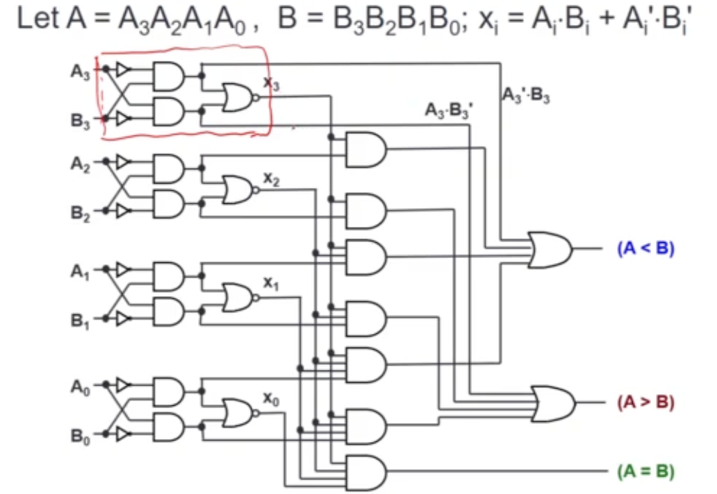
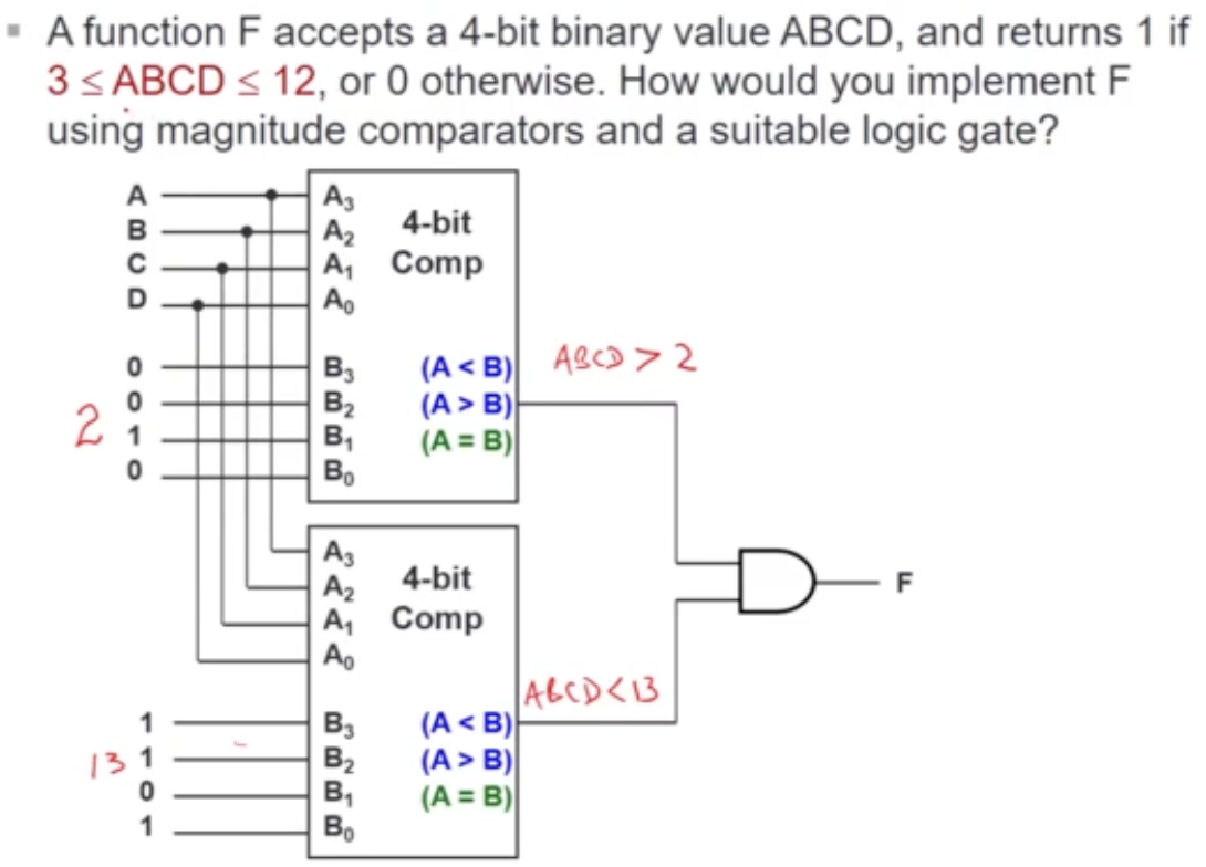
Magnitude Comparator
- compare 2 unsigned values A and B, to check if A > B, A=B, or A < B
- To design an n-bit magnitude comparator using classical method, it would require rows in the truth table
- This is simply too much!
Analysis
- if MSBA > MSBB, then A > B
- Likewise for the remaining bits
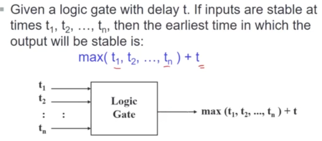
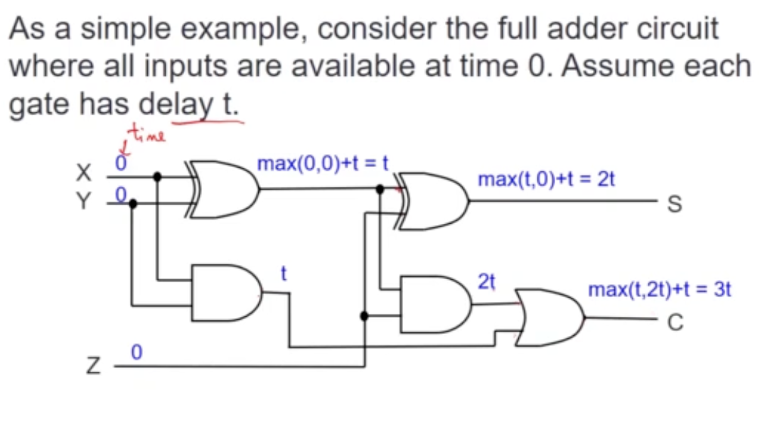
Circuit Delay
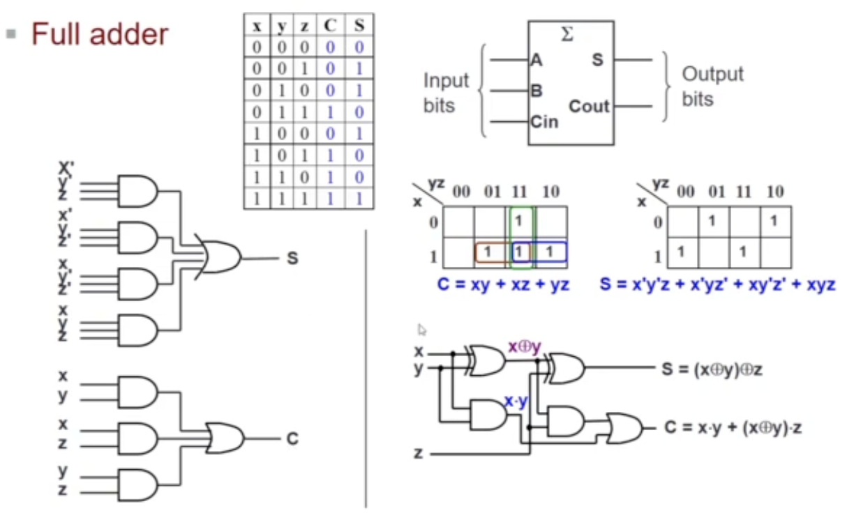
Summary of Arithmetic Circuits
Half Adder
Full Adder
4-bit parallel Adder